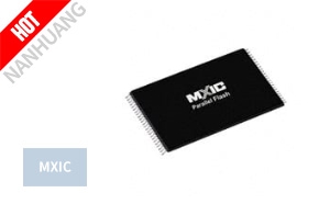
As opposed to multi-level cell (MLC) and triple-level cell (TLC) memory, single-level cell (SLC) NAND flash enables high-speed reads and writes as well as excellent reliability and therefore meets the requirements for high performance and high durability imposed by IoT devices, automotive electronics and emerging embedded applications. However, amid fierce market competition, the ability to maintain a cost advantage continues to play an instrumental role in a product's success. Memory manufacturers have been leveraging progress in miniaturization of semiconductor integrated circuits to help them keep costs down and stay ahead of the competition.
Psyche Kuo, deputy director of product marketing at Macronix International, noted that as a leading manufacturer of nonvolatile memory solutions for three decades, Macronix has accumulated extensive experiences in the volume production of SLC NAND, making its way onto the list of the world's top three SLC NAND suppliers. Its outstanding track record in SLC NAND applications in embedded systems, on top of its excellent product quality and production capacity, has enabled Macronix to win support from system integrators and its memory spec to become mainstream standard used in wide-ranging embedded systems. To stay on top of market demand, Macronix has again introduced new-generation SLC NAND solutions produced on the 19nm node, taking advantage of advanced semiconductor process technologies.
In full control of production with its own fabrication facilities, Macronix boosts customer satisfaction
Macronix expects the family of 19nm SLC NAND products to become a major pillar supporting its 2020 revenue. The 19nm SLC NAND family comprises two subgroups: SLC NAND featuring full support for the Open NAND Flash Interface (ONFI) and Serial NAND. They target niche application markets including smart speakers, set-up boxes, streaming TV, smart home devices and other high-profile electronics, as well as niche high-end network communication products such as broadband network access equipment. Satisfying customer needs in memory capacity and cost, Macronix's 19nm SLC NAND will further strengthen its leading position in the embedded memory market.
First and foremost, Kuo pointed out that embedded system customers attach great importance to product quality and supply stability. Macronix operates its own fabrication facilities and thus is in control of production capacity. It is capable of planning production capacity to accommodate customers' shipment schedule. With a proven track record of shipping billions of chips and years of experience in volume production, Macronix is able to maintain long-term relationships with brand customers based on the guarantee of supply stability and agile production planning.
As it moves to advanced technology, the SLC NAND naturally will require a host controller to handle stronger error correction code (ECC). Macronix's 19nm SLC NAND requires the same 8-bit ECC as other 2x-nanometer SLC NAND in the industry now, which is the mainstream specification. Additionally, the Macronix family provides tailored features to satisfy more needs to customers in niche markets.
Macronix taps growing niche markets with a diversity of new product features
Aside from ECC requirement following the mainstream specification, the new SLC NAND is the first to come with a unique ID (UID) based on the "physical un-clonable function" (PUF), which comes from cell characteristic and it is truly random and un-predictable. Macronix's new 19nm SLC NAND components allow for checking the authenticity of a memory component to make sure it has not been swapped with an unauthorized one. The UID can be retrieved using a read-unique ID command. The microcontroller can compare the read-out of the ID with the original one stored in a safe area.
The new SLC NAND also features randomizer function, which is especially for a special data pattern, such as extreme an unbalance data pattern on the distribution of zeros and ones. For NAND read interference caused by errors in this kind of case, this function is used to pre-transform the data into evenly distributed zeros and ones and to resolve the risk of data being read inaccurately.
In addition, the NAND memory is susceptible to the Read Disturb effect due to highly intensive and frequent reads - a situation that can easily cause read data errors after high-intensive frequent erasure and data modification (Program Disturb), as well as long-term data retention requirements. In response to these situations and high-quality reliability requirements, a special read function named the Special Read for Data Recovery is provided in the Macronix 19nm SLC NAND for data recovery. This function can adjust the internal condition of NAND FLASH, and may save data and extend the memory lifetime from that. These new features effectively reduce errors during data reading, improve system stability, and meet the stringent requirements of embedded systems for data access applications.
Shipments of the 3V 4Gb model began in the fourth quarter of 2019 with 1/2/8Gb devices to follow in the first quarter of 2020. Macronix is also preparing to launch of 1.8V 19nm SLC NAND. Kuo has high hopes for the 3V product family due to large market demand and the wide range of embedded system applications needing SLC NAND, especially those running Linux OS. Macronix is envisioning large orders going forward into 2020.
19nm SPI NAND flash with cost advantage allows processors to maximize their benefits
Macronix's 19nm SPI NAND series is positioned as niche and high-value-added products. As CPU manufacturers scramble to add powerful computing cores to cope with the demand of smart Automotive Internet of Things (AIoT) applications, equipping CPUs with 8-bit, 12-bit or even higher ECC capability is becoming standard in the market. In view of this, processing of ECC by the memory is inefficient, while ECC-related specifications vary among memory vendors, thus posing problems for microcontrollers to adopt ECC. Macronix specifically removed the built-in ECC function of 19nm SPI NAND memory products, allowing customers to fully enjoy the high-performance advantage of cost and processor control, in line with its strategy to move toward customization and cater to market demand.
Macronix regards satisfying leading semiconductor firms as its top priority. Moreover, as 19nm chips are smaller and therefore can better accommodate different system-in-package (SiP) designs by leading semiconductor firms, a wide variety of customized semiconductor solutions can be made through with them. Major system chipmakers can use a stack of different density memory chip with logic chips or processors to integrate some customized semiconductor solutions. As leading vendors, Macronix is the first to launch a complete solution for 19nm SLC NAND memory, which takes an important step forward in embedded applications and helps international brands to expand the markets for smart devices, smart communication and AIoT systems.
All registered trademarks and other trademarks belong to their respective owners. For more details, please visit MXIC(Macronix) official site.
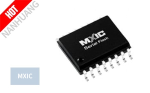
- IC FLASH 64MBIT SPI 86MHZ 16SOP
- IC FLSH 128MBIT SPI 104MHZ 16SOP
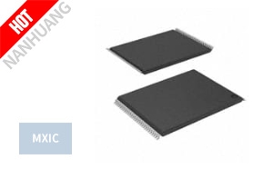
- IC FLASH 512MBIT PARALLEL 56TSOP
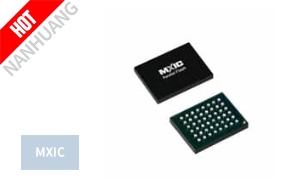
- IC FLASH 8MBIT PARALLEL 48LFBGA
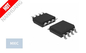
- IC FLASH 128MBIT SPI 120MHZ 8SOP
- IC FLASH 4GBIT PARALLEL 48TSOP
- IC FLSH 128MBIT SPI 104MHZ 16SOP
- IC FLASH 8GBIT PARALLEL 48TSOP
- IC FLASH 256MBIT SPI/QUAD 16SOP
- IC FLASH 4MBIT SPI 86MHZ 8SOP
- IC FLASH 2GBIT PARALLEL 48TSOP
- IC FLASH 64MBIT PARALLEL 48TSOP
- Macronix is introducing the second-generation ULV 1.2V SPI NOR flash product line in 2020 to meet th
- Macronix is contemplating a US$1.5 billion expansion after 2021
- Macronix's 19nm SLC NAND will further strengthen its leading position in the embedded memory market
- Macronix will start volume shipments of its own 3D NAND memory in the second half of next year
- Macronix announced the sale of Macronix's 6-inch wafer plant and equipment to Foxconn for NT $2.52 b
- Macronix plans to expand 12-inch wafer capacity for advanced 3D NAND and NOR flash memory chips


